**The AD7533JPZ: A Comprehensive Technical Overview of the Monolithic 10-Bit Multiplying DAC**
In the realm of precision digital-to-analog conversion, the **AD7533JPZ** stands as a significant and enduring component. This monolithic, 10-bit multiplying digital-to-analog converter (DAC) from Analog Devices has been a cornerstone in applications requiring high accuracy and versatile signal manipulation. Its architecture and functionality offer a masterclass in efficient, reliable digital-to-analog conversion.
At its core, the AD7533JPZ is a **current-output, multiplying DAC** built on a monolithic CMOS process. The "multiplying" capability is its defining characteristic; unlike fixed-reference DACs, its output signal is the product of a digital code and an analog input reference voltage. This allows it to function not just as a simple DAC but also as a **programmable attenuator**, a digital potentiometer, or a key component in complex analog modulation schemes. Its 10-bit resolution provides 1,024 discrete output levels, ensuring a fine enough granularity for a wide array of control and measurement applications.
The internal architecture of the AD7533JPZ is comprised of a precision R-2R ladder network, a group of NMOS current switches, and a data latch for each bit. The R-2R ladder is renowned for its ability to ensure monotonicity, a critical feature where the output analog voltage always increases for an increasing digital code, preventing errors during transitions. The onboard latches are crucial for stability; they hold the digital input word, allowing the DAC to update its output state only when the user commands it via the load signal, thus preventing spurious output glitches during the data loading process.

A key advantage of this DAC is its **four-quadrant multiplication** ability. The polarity of both the reference voltage (VREF) and the resulting output current can be positive or negative. This enables the device to handle AC signals and operate in all four quadrants of the coordinate plane, making it indispensable for applications like complex waveform generation, automatic gain control, and sine/cosine function synthesis.
The AD7533JPZ requires external operational amplifiers to convert its high-impedance current output into a low-impedance voltage output. This external configuration provides designers with flexibility. By choosing amplifiers with specific speed, noise, and precision characteristics, the overall circuit performance can be tailored to the application's exact needs, ranging from DC precision to higher-speed signal processing.
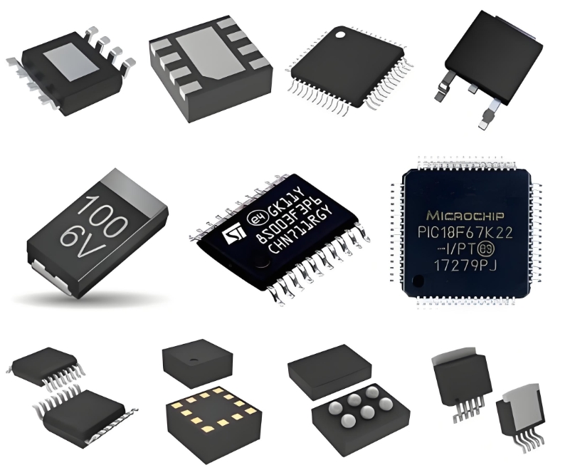
Housed in a 20-pin plastic DIP (PDIP) package, the AD7533JPZ is designed for robustness and ease of prototyping. Its specifications include **low power consumption**, typical of CMOS technology, and low gain error, which simplifies calibration and system design. While modern designs might opt for newer DACs with higher resolution or integrated output amplifiers, the AD7533JPZ remains a benchmark for understanding fundamental DAC operation and for use in systems where its specific combination of features is optimal.
**ICGOOODFIND**: The AD7533JPZ is a quintessential example of a versatile, monolithic multiplying DAC. Its enduring value lies in its robust R-2R architecture, four-quadrant multiplication capability, and the design flexibility offered by its current-output structure, cementing its place as a fundamental building block in precision analog electronics.
**Keywords**: Multiplying DAC, Monolithic CMOS, R-2R Ladder, Four-Quadrant Multiplication, Current Output.
